Day 1: May 12th | Afternoon

Welcome note

13:45 – 14:00

Welcome, Horizon Europe ICOS: EU and non-EU Strenghts, Weaknesses, Dependencies, Opportunities for International Collaboration  Francis Balestra, ICOS Coordinator, Grenoble INP/CNRS/ SiNANO Institute

Francis Balestra, CNRS Research Director at CROMA, is Director Emeritus of the European SINANO Institute and President of IEEE Electron Device Society France, and has been Director of several Research labs. He coordinated several European Projects (NEREID, NANOFUNCTION, NANOSIL, etc.) that have represented unprecedented collaborations in Europe in the field of Nanoelectronics, and is currently coordinator of the Horizon Europe ICOS project dedicated to International Cooperation on Semiconductors with leading semiconductor countries.

He founded and organized many international Conferences, and has co-authored more than 500 publications.

He is member of several European Scientific Councils, of the Advisory Committees of International Journals and of the IRDS (International Roadmap for Devices and Systems) International Roadmap Committee, as representative of Europe.

The main objectives and outcomes of the Horizon Europe project ICOS dedicated to International Cooperation on Semiconductors will be presented. International cooperation is key for speeding up technological innovation, reducing cost by avoiding duplicated research, boosting the resilience of the semiconductor value and supply chains, and is one of the objectives of the EU Chips Act. The main ICOS results dealing with the analysis of the semiconductor economic and technological landscapes in Europe and leading semiconductor countries, as well as the identification of areas of potential cooperation on advanced functionalities and computing will be highlighted.

Session 1 – Turn risks into chances: closing gaps in the semiconductor value chain

14:00 – 17:00

– Interactive session: Turn risks into chances: closing gaps in the semiconductor  value chain – Melanie Hentsch, Sven Bökemeier, Monika Curto Fuentes (VDI VDE), Beth McEvoy (Future of UK Semiconductor R&D – UKRT Grant)

Monika Curto Fuentes studied International Law and International Relations at the Adam Mickiewicz University in Poznan, Poland and the University of Bielefeld, Germany. She has been working as a scientific advisor for mobility, energy and future technologies at VDI/VDE-IT since 2017. Ms. Curto Fuentes accompanies various European projects in the field of battery cell production (Batteries Europe, Battery IPCEI and Battery2030+) and semiconductors (ICOS), in which she is responsible for the international monitoring of battery and semiconductors ecosystems and the benchmarking of international KPIs.

Sven Bökemeier completed his double degree with a focus on thin films in Science and Technology of New Materials at the University of Seville and Physics at the University of Münster. In 2023, he began his role as a scientific consultant at VDIVDE-IT in the field of microelectronics and high-performance computing, where he serves in addition to his work on the ICOS project as a consultant for the Federal Ministry of Education and Research and accompanies national and international projects in various parts of the semiconductor value chain.

Beth McEvoy is a strategic foresight practitioner, working at the intersection of anticipation studies and systems thinking. An expert in transdisciplinary research programmes, she is Research Co-Investigator on the UKRI Future of Semiconductor R&D project, the manager of the eFutures electronic systems network, and a named specialist on a major project that re-imagines the supply chains of tomorrow. In the city of Belfast, she currently works on the future of urbanity, sustainable placemaking, and tech for societal good.

This session is co-organised with the project Future of UK Semiconductor R&D, funded as part of the UKRI grant and commissioned by DSIT.

International cooperation is a key objective of the ICOS project. By encouraging diverse perspectives, we can develop actionable strategies to achieve this goal.

The interactive workshop will engage participants in group discussions to identify main gaps in the European semiconductor value chain and explore solutions to turn risks into opportunities.
Through collaborative brainstorming and strategic foresight methodologies, we will focus on measures needed in critical areas such as advanced materials, packaging technologies, design methods, and AI-driven innovations.

Join us to contribute your insights and shape the future of Europe’s semiconductor industry!

 Coffee Break 17:00 – 17:30

Session 2 – Standardisation

17:30 – 19:00

– Standardisation session. – Working Group StandICT.eu / AllPros.eu / ICOS

This session is co-organised with ALLPROS.EU and StandICT.eu.


Silvana Muscella, Founder & CEO of a dynamic SME Trust-IT Services, and co-founder of a software house COMMPla Srl based in Tuscany, Italy, where we support private and public companies in their digital processes. Currently the project coordinator of the DEP CSA, ALLPROS.eu, which supports the Secretariat of the Industrial Alliance of semiconductors and microprocessors. Over 25 years’ experience on ICT on high-level strategy & policy building, business acquisition, coordination & strategic marketing and communication developments in ICT in standards

Served as coordinator of some major EU projects that have impacted efforts around ICT standards, being the coordinator of the pilot project StandICT.eu for over 5 years now in its 4th edition. Expert Evaluator, Reviewer, to evaluation & assessment panels regularly engaged, since 2003 by the European Commission. Chair of 2nd High-Level Expert Group HLEG EOSC -European Open Science Cloud [2017-2018] & co-author of Prompting an EOSC in Practice

Abstract

ICT Standardisation Evolutions & Impact in the EU Landscape

The talk will zoom in on the evolution of the different European funded efforts around ICT Standardisation that has taken place in Europe for the past 8 years, largely through the example of the successful community driven CSA – StandICT.eu project. Moreover, the talk will also touch upon some impactful results and recommendations around how Europe could strengthen its role in ensuring standards are aligned to market needs. Efforts we are doing within the semiconductor industry space and how technical working group work between ICOS, StandICt.eu & ALLPROS.eu as well as touching upon the growth of Women in ICT Standards which we’d like to explore further in 2025 & the new edition of StandICT.eu 2029.

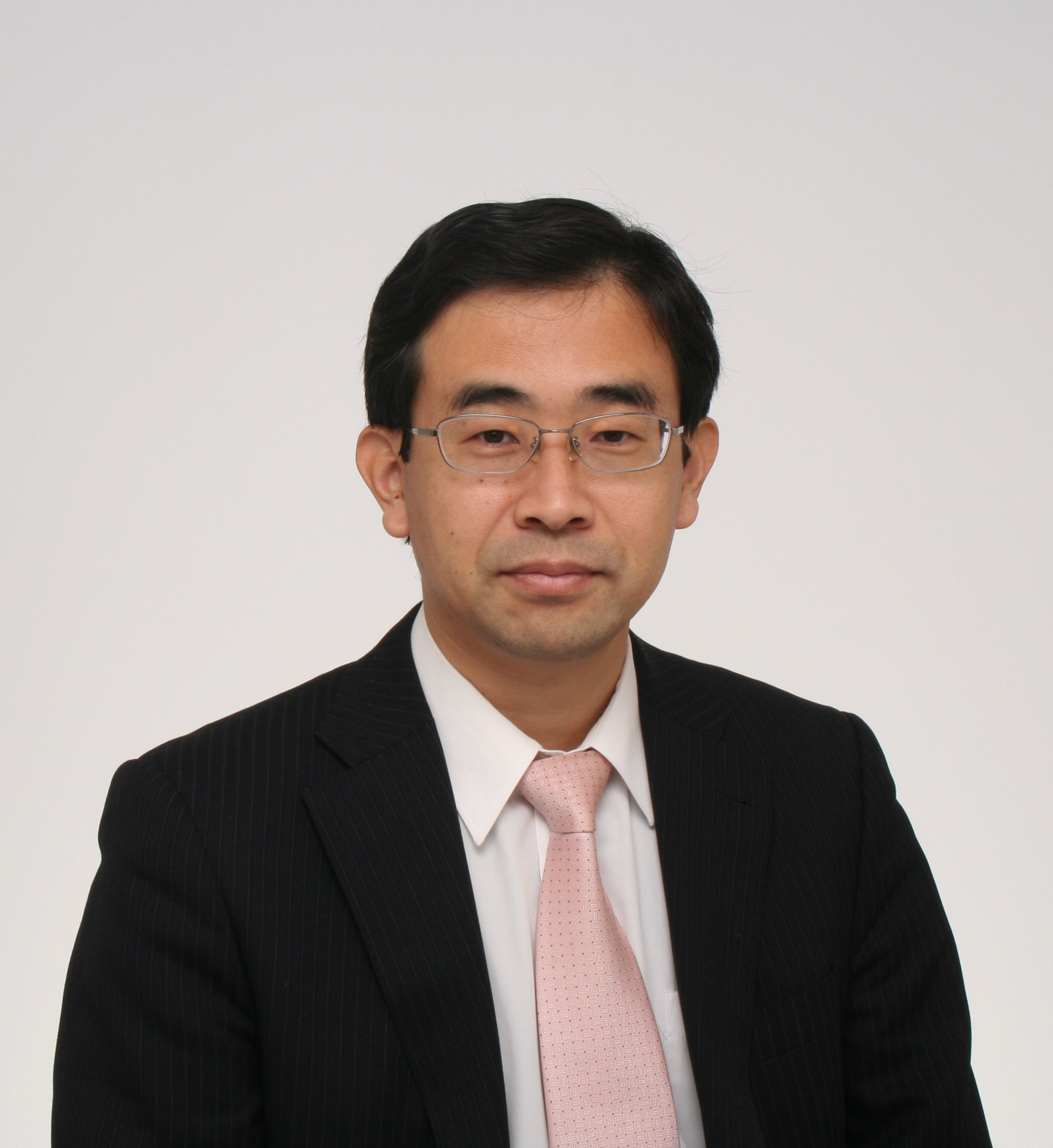
Hiroyuki Akinaga (Senior Member, IEEE) received the B.E., M.E., and Ph.D. degrees from the University of Tsukuba, Ibaraki, Japan, in 1987, 1989, and 1992, respectively. He worked at the National Institute of Advanced Industrial Science and Technology (AIST) from 1992 to 2025, including as director of the Nano Device Center. He is currently a professor at the Faculty of Information Science and Technology, Hokkaido University. He is co-leader of the Beyond CMOS Working Group (WG) at International Roadmap for Devices and Systems (IRDS), Japanese leader of the research field of energy harvesting at More-than-Moore WG, and a strategic committee member at WG of Environment, Health, Safety and Sustainability (ESHS). He has been serving as a convenor at International Electrotechnical Commission (IEC), TC113 (Nanotechnology for electrotechnical products and systems), WG7 (Reliability) and WG13 (Wafer-Scale System Integration). He is a fellow of Japan Society of Applied Physics. His current interests include nanoelectronics and open innovation platforms.

Abstract:

Standardization to promote international cooperation in nanoelectronics

As a long-term expert-driven mechanism for international research cooperation, I would like to introduce the activities of roadmapping and standardization. These cooperations act as both wings of a bird to promote research and development. The international standardization activities in International Electrotechnical Commission (IEC) Technical committee (TC) 113 (Nanotechnology for electrotechnical products and systems) are shown as the practical example and evaluated in comparing to the international roadmap activities. On the other hand, from the perspective of roadmapping, I would like to introduce the concept of “Green material”, which maintains sustainability in semiconductor manufacturing, and discuss the role of international standardization in advancing sustainable practices [1].

[1] A. Ueda, H. Akinaga, S. Agarwal, J. A Hagmann, S. Das, M. J Marinella and A. Chen, “Green materials in semiconductors: perspective from the IRDS beyond-CMOS roadmap”, Nanotechnology 36, 142001 (2025),

https://iopscience.iop.org/article/10.1088/1361-6528/adb041.

19:00 Networking cocktail

 Day 2: May 13th | Morning

Session 3 – EU International Cooperation on Semiconductors: Opportunities and Challenges

8:45 – 12:00

– EU International Cooperation on Semiconductors: Opportunities and Challenges.
 Chairs: Paolo Motto Ros, Danilo Demarchi (Politecnico di Torino), Giorgos Fagas (Tyndall National Institute)

Giorgos Fagas PhD MBA is Head of CMOS++ and EU Programmes at Tyndall, and member of Tyndall’s Leadership Team. CMOS++ is a strategic programme addressing emerging materials, devices and architectures for next-generation information processing interfacing with CMOS and beyond. He is contributor to key international strategic R&I agendas incl. the ECS-SRIA and IRDS and has initiated several large-scale EU projects. He currently leads the EU-funded programmes for open access to infrastructure for early-stage research on nanoelectronics and semiconductor chips, respectively, ASCENT+ and INFRACHIP, and the ICOS project activity on Technology Scanning and Foresight. Giorgos holds prominent positions in various policy and industry groups including Director of the SiNANO Institute.

Danilo Demarchi: Full Professor at Politecnico di Torino, Leading the eLiONS Lab (electronic Life-Oriented iNtelligent Systems). Smart System Integration and IoTs for the AgriFood Value Chain and for BioMedical Devices. Pioneer in the research on Wearable Plant Sensors.
Visiting Professor at EPFL Lausanne (2019) and at Tel Aviv University (2018-2021). Visiting Scientist (2018) at MIT and Harvard Medical School. Founder and Editor in Chief of the IEEE Transactions on AgriFood Electronics. Founder and Chair of the IEEE CAS Special Interest Group on AgriFood Electronics. 2023-2024 Distinguished Lecturer for the IEEE CAS Society with the Lecture “Let the Plants Do the Talking: Smart Agriculture by the messages received from Plants and Soil”. Founder at Politecnico di Torino of the Master’s Degree in AgriTech Engineering.

Paolo Motto Ros: Assistant Professor at Politecnico di Torino. Circuits and systems, and smart system integration, for wireless implantable and wearable biomedical devices and applications; electronics for agrifood.
Senior postdoc researcher at Istituto Italiano di Tecnologia (2014-2019) and Politecnico di Torino (2019-2022). Program co-chair of ApplePies 2024; member of the organizing committee of IEEE ICECS 2019, IEEE FoodCAS2021 (ISCAS2021), and IEEE CAFE 2023; RCM of IEEE BioCAS 2021-2024, organizer of a special session at IEEE MeMeA2021, PCM of IEEE LASCAS2022/2023; guest editor of MDPI Sensors and guest associate editor of Frontiers in Neurorobotics. Associate Editor of IEEE Transactions on Biomedical Circuits and Systems and IEEE Transactions on AgriFood Electronics.

The session aims to have contributions form non-EU leading experts about the strengths and weaknesses of seven countries (Japan, South Korea, USA, Singapore, Taiwan, India, China) in the semiconductor value chain and propose recommendations for international research cooperation.

8:55 – 9:15 Rakesh Kumar, Chair of IEEE Future Directions, DataPort, Past-chair IEEE Roadmaps, (USA)

Dr. Rakesh Kumar is a semiconductor industry veteran, an entrepreneur, and an educator. He is the founder, President and CEO of TCX Technology  Connexions. He also educates and mentors potential engineering entrepreneurs at UCSD. Dr. Kumar has authored the book “Fabless Semiconductor Implementation”, published by McGraw Hill. He is an IEEE Life Fellow and was inducted into the IEEE Technical Activities Hall of Honor in 2018. He is currently Chair of the IEEEFuture Directions, IEEE DataPort and has been President of the Solid-State Circuits Society (2012-13). He has also held numerous other leadership roles at IEEE. He was Vice Program Chair for the 2017 Sections Congress. During 40+ years in the semiconductor industry he has been VP&GM at Cadence Design, and has held various
technical and management positions at Unisys and Motorola. He received the Ph.D. M.S. and B.S diplomas in EE from the University of Rochester, and IIT Delhi, and an Executive “MBA” from UCSD.

Technology innovations over the years are being used to create engineering solutions at an increasingly rapid pace. A global supply chain has evolved to meet worldwide demands. Demands of Artificial Intelligence semiconductors have spurred the need for further technology enhancements in the semiconductor processes, packaging and design. Successful development and implementation of these semiconductors requires close collaboration between system level design, process technologies and packaging. This can be achieved through continued collaboration between entities around the globe as well as within each region. This keynote talk will provide select examples of some exciting solutions.

9:15 – 9:45  Yong Ilan, IEEE Division 1 Director, member of the IEEE Board of Directors, (China and Singapore)

9:45 – 10:05  Dr. Tuo-Hung Hou, Director General of the Taiwan Semiconductor Research Institute (TSRII), (Taiwan)

Dr. Hou received his Ph.D. in electrical and computer engineering from Cornell University in 2008. He joined Taiwan Semiconductor Manufacturing Company (TSMC) in 2000 and worked at International SEMATECH (2001–2003). Since 2008, he has been with NCTU (now National Yang Ming Chiao Tung University, NYCU), where he is now a Chair Professor and served as Associate Vice President for R&D. He currently leads the Taiwan Semiconductor Research Institute (TSRI) as the Director General. His research focuses on nonvolatile memory, neuromorphic computing, and heterogeneous integration of silicon electronics with low-dimensional and low-temperature nanomaterials. Dr. Hou has received numerous awards, including the Ministry of Science and Technology Outstanding Research Award (twice). He is an IEEE EDS Distinguished Lecturer and serves on multiple technical committees of premier international conferences.

The Taiwan Semiconductor Research Institute (TSRI), founded in 1988, stands as Taiwan’s premier government-funded hub for semiconductor innovation. Over 35 years, TSRI has grown into a global leader in IC design and manufacturing, offering advanced research platforms in CMOS, memory, 3D packaging, silicon photonics, and quantum computing. This talk explores TSRI’s pivotal role in fostering a collaborative ecosystem, uniting over 60 universities, 500+ research groups, and industry partners. By providing cutting-edge tools and training, TSRI accelerates technology development and nurtures talent, ensuring Taiwan’s semiconductor dominance. The discussion will highlight TSRI’s strategies for sustaining leadership amid global competition through international collaboration.

10:05 – 10:30 Coffee Break

10:30 – 10:50  Sunita Verm, Group Coordinator (R&D) at Ministry of Electronics & JT, (India)

Smt. Sunita Verma is the Group Coordinator for R&D in Electronics, IT and CC&BT at Ministry of Electronics & IT overseeing the entirety of R&D operations including National Supercomputing Mission (NSM). Her pivotal role extends to crafting policies, evolving R&D proposals, orchestrating their execution, and facilitating their commercialization through collaborative efforts with industrial, academic, and R&D entities. With an extensive tenure spanning over three decades, her experience spans over the spectrum of R&D endeavors, from basic research to product development in the areas of Artificial Intelligence(AI), Quantum technologies, Micro-Electronics, Nano Technologies, Electronics Material, Medical Electronic, Electronics Systems Development, Perception Engineering, Blockchain Technology, Next Generation Communication technologies like 5G, 6G and beyond, Convergent technologies, Strategic Electronics & Communication like Cognitive Radio, SDR, Tactical Communication, etc.

She is heading the National Supercomputing Mission for development & deployment of 24PF state-of-the-art Supercomputing facilities in the country, Development of RISC-V based series of indigenous Microprocessors, NavIC Receiver Chipsets etc.

She was instrumental in the development of PARAM SHAVAK machine “Supercomputer in a Box” based on indigenously developed Rudra Server Board.

She has been driving the nation-wide Specialized Manpower Development Programme- Visvesvarya PhD Scheme to enhance the PhD in Electronics and IT sectors; Chips to Start-up Progamme to train 85,000 number of industry-ready manpower at B.Tech, M.Tech and PhD level in Chip/ SoC design area; as well as; Design Linked Incentive (DLI) Scheme as part of Semicon India Policy to nurture the domestic fabless design ecosystem to develop Chips & SoCs for automotive, mobility and compute areas.


Coming soon

10:50 – 11:10  Jinwook Burm, Professor at Sogang University

Jinwook Burm earned B.S. from Seoul National University, Seoul, Korea, M.S. from the University of Michigan, Ann Arbor, and Ph.D. from Cornell University, Ithaca, NY. After completing postdoctoral work at Cornell University and Bell Labs, Lucent Technologies, Murray Hill, NJ, he joined the Department of Electronics Engineering at Sogang University, Seoul, Korea, as an Assistant Professor in 1998. He is currently a Professor at Sogang University. He is currently engaged in various research projects, including high-speed CMOS interface circuits, sensors, and neuromorphic circuits. His roles in various conferences include General Chair of ISOCC 2015, General Co-Chair of ISCAS 2021 in Daegu, Korea, and General Co-Chair of ISICAS 2023 in Jeju, Korea. In 2021, he served as the president of the Institute of Semiconductor Engineers, a Korea-based semiconductor society. He is currently a Board of Governors member at large of CASS for the term 2025-2027.


The strengths and weaknesses of semiconductors in Korea

South Korea is a global leader in the semiconductor industry, home to major companies like Samsung and SK Hynix. Strengths include advanced fabrication technology, strong government support, and dominance in memory chips, particularly DRAM and NAND flash. Additionally, a well-established supply chain and skilled workforce contribute to its competitiveness. However, weaknesses remain, such as heavy reliance on a few key players, limited presence in logic chips and foundry services compared to TSMC, and vulnerability to global supply chain disruptions. Increasing geopolitical tensions and dependence on foreign semiconductor equipment and materials further challenge Korea’s long-term semiconductor industry sustainability and growth.

11:10 – 11:30 Hiroyuki Akinaga, University of Hokkaido / National Institute of Advanced Industrial Science and Technology (AIST)

Hiroyuki Akinaga (Senior Member, IEE) received the B.E., M.E., and Ph.D. degrees from the University of Tsukuba, Ibaraki, Japan, in 1987, 1989, and 1992, respectively. Currently, he is the Principal Research Manager, Device Technology Research Institute, National Institute of Advanced Industrial Science and Technology (AIST). He is co-leader of the Beyond CMOS Working Group (WG) at International Roadmap for Devices and Systems (IRDS), Japanese leader of the research field of energy harvesting at More-than-Moore WG, and a strategic committee member at WG of Environment, Health, Safety and Sustainability (ESHS). He has been serving as a convenor at International Electrotechnical Commission (IEC), TC113 (Nanotechnology for electrotechnical products and systems), WG7 (Reliability) and WG13 (Wafer-Scale System Integration). He is a fellow of Japan Society of Applied Physics. His current interests include nanoelectronics and open innovation platform

11:30 – 12:00 Panel of Experts

12:00 – 14:00 Lunch Break

 Day 2: May 13th | Afternoon

Session 4 – Opportunities of international cooperation in the emerging technologies landscape


14:00 – 14:30

– Opportunities of international cooperation in the emerging technologies landscape. Giorgos Fagas (Tyndall National Institute)

Giorgos Fagas PhD MBA is Head of CMOS++ and EU Programmes at Tyndall, and member of Tyndall’s Leadership Team. CMOS++ is a strategic programme addressing emerging materials, devices and architectures for next-generation information processing interfacing with CMOS and beyond. He is contributor to key international strategic R&I agendas incl. the ECS-SRIA and IRDS and has initiated several large-scale EU projects. He currently leads the EU-funded programmes for open access to infrastructure for early-stage research on nanoelectronics and semiconductor chips, respectively, ASCENT+ and INFRACHIP, and the ICOS project activity on Technology Scanning and Foresight. Giorgos holds prominent positions in various policy and industry groups including Director of the SiNANO Institute.

Coming soon

Session 5 – International cooperation for a resilient Europe: priorities and opportunities


14:30 – 15:00

– International cooperation for a resilient Europe: priorities and opportunities. Mattias Verstuyft (ePIXfab/ UGent)

Mattias Verstuyft got his master thesis in theoretical physics at the University of Ghent in 2016, after which he did a PhD in silicon photonics at the Photonics Research Group in Ghent University under prof. Bart Kuyken. After managing several EU funded photonics projects with industrial and academic partners (through ActPhast and PhotonHub Europe), he started working as the technical coordinator of ePIXfab – the European silicon photonics alliance – where he handles day-to-day operations, coordinates trainings and other activities, and advocates on behalf of its members and the silicon photonics community at large.

We will present an analysis of the most urgent challenges facing the European semiconductor field and identify opportunities for international cooperation with other regions. This analysis is based on a survey polling experts in the field as well as previous work done in ICOS. We will finish by requesting feedback and opinions on this analysis from the audience.

Session 6 – The emerging value chains according to the development of partnerships

15:00 – 15:40

– The emerging value chains according to the development of partnerships. Krzysztof Mieszkowski, (CEZAMAT WUT)

Krzysztof Mieszkowski is a researcher at the Centre for Advanced Materials and Technologies CEZAMAT at Warsaw University of Technology. He holds a master’s degree in finance and banking from the Warsaw School of Economics. He has almost 20 years of professional experience in the field of scientific research and development and higher education, including aspects of research and innovation policy.  His portfolio of recent projects includes ERA_FABRIC, ICOS, Mazovia EDIH, INFRACHIP and FAMES. From 2012 to 2019, he worked at the European Commission’s Joint Research Centre in Seville. As a member of the Smart Specialisation team, he was involved in promoting and implementing the concept of smart specialisation. That time, he also dealt with the Key Enabling Technologies theme and in the activities of the Thematic Platform on Smart Specialisation for Industrial Modernisation. In 2005-2012 he worked at the Ministry of Science and Higher Education in the department responsible for the implementation of the Structural Funds and in the strategy department. He contributed to the analysis of science and higher education policy issues. He used to be a member of working groups of the European Commission and the OECD.

16:00 – 16:30 Coffee Break

Session 7 – Panel Session “Potential international collaborations on emerging semiconductor technologies”

16:30 – 17:45

Dr. Peter Ramm is head of Strategic Projects at Fraunhofer EMFT Munich, responsible for initiation and steering of strategic projects and international research co-operations. He received Masters and PhD degrees from the University of Regensburg and subsequently worked for Siemens in the DRAM facility where he was responsible for the overall process integration. In 1988, he joined Fraunhofer, focusing for more than 35 years on 3D integration technologies. Ramm developed and patented 3DIC approaches with particular focus on heterogenous integration. Peter Ramm is author of over 130 publications and 30 patent families. He received the “Ashman Award 2009” from IMAPS and the 2020 IEEE Technical Field Award “For Pioneering Contributions Leading to the Commercialization of 3D Wafer and Die level Stacking Packaging”.
Peter Ramm is Senior Member IEEE, IMAPS Fellow and Life Member.

The renowned panelists from universities, RTOs and industry will identify and discuss critical needs for future semiconductor technologies. The main goal is to identify emerging opportunities for international R&D initiatives/collaborations/partnerships – with the feedback of the audience.

Key technological challenges to be discussed are in the fields of More Moore, Beyond CMOS and More than Moore, as – but not limited to – CMOS scaling, advanced patterning technology, RF devices, memory, power devices, sensing technologies & MEMS, FDSOI, 2D materials, quantum computing, neuromorphic computing, heterogeneous integration, advanced packaging and microelectronics assembly.

Hiroyuki Akinaga (Senior Member, IEEE) received the B.E., M.E., and Ph.D. degrees from the University of Tsukuba, Ibaraki, Japan, in 1987, 1989, and 1992, respectively. Currently, he is the Principal Research Manager, Device Technology Research Institute, National Institute of Advanced Industrial Science and Technology (AIST). He is co-leader of the Beyond CMOS Working Group (WG) at International Roadmap for Devices and Systems (IRDS), Japanese leader of the research field of energy harvesting at More-than-Moore WG, and a strategic committee member at WG of Environment, Health, Safety and Sustainability (ESHS). He has been serving as a convenor at International Electrotechnical Commission (IEC), TC113 (Nanotechnology for electrotechnical products and systems), WG7 (Reliability) and WG13 (Wafer-Scale System Integration). He is a fellow of Japan Society of Applied Physics. His current interests include nanoelectronics and open innovation platform

Mustafa Badaroglu works at Qualcomm with focus on technology ramp and architecture enhancements of AI chipsets, ultra-low voltage process and design methods and stacked memory technologies. Before joining Qualcomm, he previously worked at Huawei, imec, ON Semiconductor, and Tubitak Space. During his career he had various assignments for the execution and management of mobile and automotive chipset design from concept to initial ramp, process technology pathfinding, and system technology co-optimization. He holds a PhD in electrical engineering from the Catholic University of Leuven in Belgium

Giorgos Fagas PhD MBA is Head of CMOS++ and EU Programmes at Tyndall, and member of Tyndall’s Leadership Team. CMOS++ is a strategic programme addressing emerging materials, devices and architectures for next-generation information processing interfacing with CMOS and beyond. He is contributor to key international strategic R&I agendas incl. the ECS-SRIA and IRDS and has initiated several large-scale EU projects. He currently leads the EU-funded programmes for open access to infrastructure for early-stage research on nanoelectronics and semiconductor chips, respectively, ASCENT+ and INFRACHIP, and the ICOS project activity on Technology Scanning and Foresight. Giorgos holds prominent positions in various policy and industry groups including Director of the SiNANO Institute.

Dominique NOGUET holds an engineering degree in electrical engineering (1992) and a PhD in microelectronics (1998). He started his carrier as an IC designer. He led many projects at a national level and in several European frameworks. He has been a key member of several IEEE standard groups in the field of Cognitive Radio. In parallel, he held managerial positions at CEA-Leti as lab manager and department manager. In January 2023, he was appointed project manager for the ‘France 2030’ flagship project NextGen on FD-SOI advanced nodes, and is currently the project coordinator of the Chips Act’s FAMES Pilot Line.

Mikael Östling received his MSc and the PhD degrees from Uppsala University, Sweden. He was deputy president of KTH between 2017-2022. His research interests are nanoscaled Si and Ge device technologies and emerging 2D materials, as well as device technology for wide bandgap semiconductors for high power/high temperature applications. He has supervised 47 PhD theses work and co-authored 500+ scientific papers published in international journals and conferences. Östling was an editor of the IEEE Electron Device Letters 2005-2014 and editor in chief of the IEEE J-EDS 2016-19. Östling is a Fellow of the IEEE.

Grzegorz Janczyk (Łukasiewicz-IMiF) graduated with honors from Warsaw University of Technology, Faculty of Electronics and Information Technology in 2000. In 2005 he was awarded a PhD in technical sciences in microelectronics at the same University.
He was assistant professor at the Institute of Microelectronics and Optoelectronics (IMiO) in Warsaw University of Technology since 2005. He is a supervisor or reviewer of numerous engineering and master theses. He was a lecturer in the field of microelectronics focused on ASIC design at the Warsaw University of Technology for over 20 years.
He joined the Lukasiewicz – Institute of Microelectronics and Photonics (Lukasiewicz-IMiF) as an assistant professor in the Department of Integrated Circuits and Systems Design in 2006. He took the position of Head of the Department of Integrated Circuits and Systems Design in 2012. Since 2024 he is the Director of Silicon Microelectronics Center in Lukasiewicz Institute of Microelectronics and Photonics covering the activities in area of silicon technology, silicon sensors development, micro assembly, characterization and ASIC and systems design in Lukasiewicz-IMiF.
For over 25 years he is involved in the field of microelectronics, microelectronic applications and founded projects development funded in domestic and international framework programs.

18:00 Visit of CEZAMAT

19: 30 Networking Dinner